Photon Energy Conversion
Photovoltaic cells (PV cells) are considered one of the most precise and efficient ways to produce electricity from the rather vague notion of photon energy. The following is a more detailed explanation of the process and some of the new trends.
Photoelectric Effect as the Primary Scheme of Photon Energy Transformation in PV Cells
The photoelectric effect lies at the heart of converting photon energy to electric voltage. As the sunlight falls onto the cell, the photons in this light with enough of electronvolt energy strip the electron ground-state pull from its atom in the cells’ semiconductor material. This yields an electric current. In 1905, the paper on the photoelectric effect by Einstein introduced the idea that one could transfer energy from a photon to an electron – a revolutionary moment in the spread of quantum mechanics and the creation of PV technologies. Unfortunately, the efficiency of such a system was never very high; however, for silicon cells, it is rather acceptable – around 15-20%.

P-N Junctions’ Electric Field
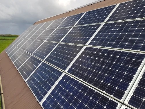
PV cells are built of the layers of silicon or another semiconductor with the P-N junction. This separates the PV cell into two parts– the free electrons’ area (n-type semiconductor), and the positive charged holes (p-type). Each of them now has an electric field on both sides directing them. The industry frequently uses silicon cells as their capacity is practicable.
Thin-Film Technology
Thin-film is a new sort of PV cells utilizing quite a small amount of photovoltaic substance. It can turn out to be more pliant and lightweight than the traditional silicon PV cells. It provides a good opportunity to integrate photovoltaics into everyday facades, such as building-integrated photovoltaics or into portable solar power equipment. According to data given by Buonicore, the efficiency of CdTe thin-film has been estimated at 22.1%, which is considerable enough for commercial use.
Multi-junction Cells
Multi-juction PV cells in their description are composed of several and several layers of semiconducting material. Each layer is designed to be the most appropriate for eliciting the desired wavelength absorptions. In the groups, the theoretical efficiency may go far beyond 45%. For use in concentrated photovoltaic systems and space, it is a choice worth considering.
Concentrated Photovoltaics
The system is there to focus the sunlight with the help of either lenses or mirrors before it reaches the PV cell. This way, the light intensity is induced steeply, and, hence, the electric voltage released. For it to function, rather precise alignment and tracking systems have to be installed. Looking at the existing systems aligned perfectly, we may notice the efficiency rates up to 46%.
Quantum Dots
Quantum dots are nanometer-sized semiconductor particles. Their inclusion in the PV cells provides a wider extent of wavelengths’ sensitivity and absorption and, hence, an improved level of the cell efficiency in absorbing and converting the light into electricity. The time comes for high-efficiency low-cost level cells – some of the quantum-based have shown even higher than 16% efficiencies.
The Role of Semiconductor Materials
The efficacy and operability of photovoltaic cells greatly rely on the type of semiconductor materials used. These materials are the core of the conversion of sunlight into electric energy. The following investigation will delve into the peculiarities of each and in what way they are applied in photovoltaic technology.
Silicon: Photovoltaics Bestie
One of the mostly widely used semiconductor materials is silicon. It is cheap and has favorable electronic characteristics. Most of the solar cells can be divided into monocrystalline and polycrystalline. The former has higher efficiency and can go up to 22%. On the contrary, the polycrystalline one generally operates from 15 to 18 but is quite cost-effective.
Real-world example: On the west coast of the United States, more than 1.7 million monocrystalline panels have been installed within Solar Star projects. They generate 579 megawatts that suffice for 255 thousand homes.
Thin-Film Materials: Maneuvering Light Energy
Thin-film photovoltaic cells utilize semiconductor materials like Cadmium Telluride and Copper Indium Gallium Selenide along with amorphous silicon. They are applied by being placed on glass, plastic, or even metal substrates. For example, the CdTe one generally has an efficiency of 22%, which is equal to silicon cells.
Real-world example: The CdTe modules performed by First Solar are generally utilized for utility-scale activities. The project-taking photo shows the efficiency and practicality of the material.
Emerging Materials: Leading-The-Way
Perovskites garnered attention due to their efficacy and low-cost production. The efficiency of the solar cell made of perovskite rapidly surged to 25% and more in labs. Combine it with silicon, and you manage to create tandem cells that have over 29.52% efficiency.
Real-world example: One of such companies that thrive is Oxford PV. It investigates the opportunities of tandem cells and in May this year established a new record of 29,52%.
Organic photovoltaic cells use organic molecules or polymers to perform the function of absorbing light and converting it into electric energy. Currently, its efficiency is not high, hovering around 10 to 12%. Nevertheless, the flexibility and cheap production of the material enable its application for specific purposes.
Doping Procedures in Semiconductors
Doping is a process of adding foreign materials to the semiconductors that positively affect its electric prowess. It is crucial for solar cells as the doping is what causes the generation of P and N-type regions within the P-N junction. This part is vital to form an electric field.
Example : In the silicon cells, boron is generally added to form the P-type region and F for the N-type one. As a result, it allows separating the electrons easily.
Band Gap Engineering: Effective Instigation
When it comes to mun0-junction or single junction cells, much of the sunlight energy is wasted. This has led to the usage of multi-junction with tandem cells. The band gap should be varied in this case as the light is primarily absorbed by different levels of cells.
Example : For example, copper steel, and selenium in CIGS have their compositions and ratios changed to allow band gap widening in a controlled manner.
Movement of Free Electrons
One crucial process for the generation of electricity or circuit in a photovoltaic cell is the movement of free electrons. This paper provides an in-depth analysis of how electrons are freed and sent to generate an electric circuit with real-life applications and explicit technical details.
Generation of Freely Moving Electrons via the Photoelectric Effect
In the first step of generating electricity in a photovoltaic cell, free electrons are generated into the semiconductor by photons. When the sun rays strike a photovoltaic cell, the photons possessing enough energy eject the electrons from their atomic binds in the semiconductor material. This effect of ejection is known as the photoelectric effect. Through Albert Einstein’s theoretical work, understanding of photoelectric effect explained how the effect had to be there as photons possessed quantized energy that could set free the electrons.
Formation and Integral Significance of Electron-Hole Pairs
In the process of freeing the electrons, electron-hole pairs are formed and spread into the p-n junctions. In is essential to differentiate the two poles as many electrons may end and spread randomly between the P-type and the N-type. However, while the free electron exists and can move by itself, it would not form electricity without the existence of positively charged “hole” left by the free electron. Thus, it is the hole that the free electron “is attracted to the hole through the electrostatic attraction, pulling it away and creating electrical current ”. In the silicon solar cell, a photon produces electron-hole pairs when energy exceeds 1.1 eV, which is the band gap of silicon.
Example: In commercial silicon solar cells, for once square meter of these cells, 200 watts of power get to be produced by the cell through sunlight. This amount to millions of electron-hole pairs generated and spread to form electricity in one square meter for a second.
P-N Junction
This area holds both pairs well and is a transmitter of these electron-hole pairs. To force electrons and holes apart, the cell must be doped to form the regions which separate electrical charges: the P-type and the N-type. The P-N junction created creates an electric field which keeps the two charges separated in what is called the separation of charges. This electric field works like a diode that allows movement of only electrons from P’ to N at the load but not holes that will go the opposite way. Approximately 90% of the separation of charges occurs in the P-N junction in the silicon solar cell.
A flow of electric current to an external circuit
How electrons are separated, the free electrons are collected by the metal contacts located on the top of the photovoltaic cell, this allows the electrons to flow through an external circuit, thus creating a flow of electric current, direct current having flowed through the electrical devices will either power the devices or charge the batteries.
How this is measured using the fill factor
This is the ratio of the maximum power point over the theoretical power and it is used to measure how well the cell converts sunlight to electricity, silicon cells are known to have a fill factor of about 0.75 to 0.85. How can recombination losses be reduced The greatest challenge in achieving high efficiency in photovoltaic technology is the elimination of recombination of electrons and holes before they are separated by the electric field.
Recombination losses can be reduced by passivating the surface of the cell, doping the necessary materials, and using high-quality materials with low number of defects. The efficiency of the cell can be increased by about 1-2% by advanced surface passivation techniques. Real-world example: The photovoltaic industry widely uses the PERC technology, this is the addition of an extra passivation layer to the rear of the cell.
How temperature can affect the mobility of carriers, dislocation defects of the material can increase as the temperature of the cell increases and this can lead to more recombination of electrons and holes and thus lower efficiency even though the electron mobility will increase. The efficiency of silicon cells can decrease by about 0.45 C. Examples: These designs may be used since it is possible to cool the solar cells to prevent overheating, an example would be a solar farm in a hot climate.
The Formation of Charge Imbalance
One of the primary conditions in photovoltaic cells is the emergence of a charge imbalance to produce electric current. The following paper explains how such imbalance is created and what can cause it as well as provides various examples and specific details.
Initial Doping of a Semiconductor
The first stage of causation includes the doping of the semiconductor substrate which enables the emergence of various regions within a single material element. The most common semiconductor material for creating photovoltaic cells is silicon. The N-type of this substance is doped with such elements as phosphorus, which result in excess electrons. The P-type region is doped with boron, which leads to the excess of holes and their continuous generation. Such a condition creates a concentration gradient, with the excess of one type of particles.
One of the real-world examples, in this case, should be considered the creation of boron and phosphorus doped silicon for high-efficiency photovoltaic modules produced by SunPower, which had an efficiency of 22% or more. The typical concentration of doped atoms is evaluated at one dopant atom per million. Moreover, potential widths of a depletion region depend on doping levels and typically do not exceed one micrometer.
Emergence of a Depletion Region
Once these P-type and N-type materials are connected there is a formation of a region called P-N junction. At this point, electrons from the N-type region start to slowly penetrate the P-type region and recombine with the holes. Therefore, the width of this depletion region has no free charge carriers and has insulator features. This development leads to the establishment of an internal electric field.
-
Photons with the energy difference between. The energy of these photons must exceed the band gap of silicon . Wherein, photons in the visible light spectrum can have energies , for which silicon is a very effective technology for generating charge carriers.
- Real-world example: at full sunlight, a typical square centimeter of a silicon solar cell can produce several hundred milliamps of current.
Separation of charges by the electric field
- The electric field inside the depletion region plays a substantial role in the isolation of the previously formed electron-hole pair. This electric Filed is strong enough to drive the electron to the N type and the corresponding hole to the P-type end, ensuring that the charges do not recombine. The strength of this electric field barely reaches 10,000 volts per centimeter. The overwhelming strength helps to overcome the thermal motion of the charge carriers. This technology exists with great efficiency to yield products of up to 23%.
Real-world example: through the effective use of the electric field for the separation of both the electrons and holes, the efficiency of the silicon cells’ panels in producing energy reaches 23%, as in the case of the Panasonic company.
Collection of charges at metal contacts
-
-
As earlier indicated, the electron-hole pair mob over to the edges in a short while and are collected by the metal contacts placed at the top and the bottom of the photovoltaic cell. Some of the charge carriers meet at these metal contacts and are swiftly channeled through the silicon towards the electron’s terminal. The basic function of these metal contacts is to ensure that the maximum amount of light does not waste in passing through while in a strong space not allowing electric carriers to freely leave. The typical element used in this design is aluminum and silver.
-
Real-world example: in contrast, the design room of Solar roof created by Tesla was properly vented and metal contacts engineered for higher optical absorption and still retained an aesthetically appealing design to the point of incorporating Bermuda’s residential roof.
Effect of keeping the charge imbalance
To ensure that the charge imbalance is maintained and electricity generation continues, the photovoltaic cell must stay in sunlight. The efficiency of the cell in maintaining the adverse charge imbalance on its sides is a function of temperature, quality of the photovoltaic material, and the precision of the manufacturing processes. Good silicon cells, for example, experience an efficiency degradation rate of less than 0.5% a year and can operate continuously for over 25 years. For instance, in long term reports by the National Renewable Energy Laboratory, it is shown that well maintained solar installations have been able to operate efficiently for over 25 years.

Current Flow in a Circuit
It is the final stage in the conversion of sunlight to usable electrical power. It describes the component, layout, and description of the photovoltaic circuit which is characterized by its real-world examples and accurate technical information.
Generation of Photocurrent
When light strikes a photovoltaic cell, electron-hole pairs are generated in the semiconductor material. The internal electric field accelerates these charge carriers which separates at the P-N junction.
Movement of majority carriers to N -type
The electric fields of the N-type layer are sufficiently strong that they force electrons by virtue of the drift and diffusion process to cross the junction and combine with the holes on the P-type layer. The typical current density of silicon solar cells under standard test conditions is around 35-40 mA/cm² [16].
Real-world example:The large-scale solar farm at the Noor Complex in Morocco, uses an advanced PV technology where the current generated is capable of powering more than ONE MILLION HOMES.
Movement of the Electrons to the External Circuit
The electrons collected at the N-type side are forced to the external load through the influence of metal contacts. The electrons pass through the external wiring to provide the electrical system with electricity. The high conductive of these contacts and the quality of the silicon part determine the efficiency of the movement. In high-efficiency devices, the current supplying wire along the edge of the cells is made of silver or aluminum. For modern high-efficiency devices, high-pure aluminum is used for the back contacts, the optimal choice for not impeding current where it maturesament at the front of the contacts that minimize electron-hole pair recombination lower the energy production capacity.
Example: Tesla’s solar panels feature back contact for high quality electricity production characterized with little electrical resistance.*
External Load and Current Utilization
It is the last process in the conversion of sunlight into electricity. The current supply in combined with the external load at the terminal it is derived to, such as a battery, electricity system of the homes, or the main grid, which uses the physical power in the battery to offer a range of power for other application. In a ranked system, whereby a given photo-voltaic silicon solar cell panel produce around 250 – 400 watts around given time, depending on the size and the systems used [18].
Real-world example: the town of Greensburg, Kansas, was rebuilt as a solar-powered town following a devastating tornado. Due to photovoltaic systems, all homes, schools, and businesses are powered by solar panels, effectively exemplifying current flow from such panels to the local electrical grid.
Inverter Role in AC Conversion
Photovoltaic cells harness sunlight to generate direct current, but most household appliances and the electrical grid operate on alternating current. As such, a modern photovoltaic system cannot operate without converting the sunlight-derived DC into AC – a task that is accomplished by an inverter. Modern inverters are extremely efficient, with over 95% of the DC power being converted into usable AC power.
Example: The Enphase IQ7 microinverter is commonly used in grid-connected household solar systems to convert the DC to AC and enable efficient energy management and monitoring.
Regulating Current Flow with Maximum Power Point Tracking
In order to optimize the current flow from the photovoltaic system and ensure that the maximum possible amount of sunlight is harnessed, Maximum Power Point Tracking technology is utilized. MPPT relatively frequently adjusts the electrical working point of the modules to ensure that they are being utilized to their maximum level. MPPT controllers can make the energy production system up to 30% more efficient.
Real-world example: The MPPT mechanism of the SolarEdge commercial solar system ensures that each solar panel operates at the point of maximum power production, increasing the overall energy harvest.
Integration with Electrical Grid
Regulations and safety standards for photovoltaic systems tightly control the levels of electricity that is provided to the electrical grid. As such, when the system is connected to the grid, the current must match the grid in frequency and voltage. Grid-tied inverters are capable of synchronizing the current to the grid’s voltage, and most grid-connected systems come equipped with such inverters in order to ensure their safe operation on the grid.
Example: The Ivanpah Solar Electric Generating System, a solar thermal plant in California, while designed to use sunlight to heat water for the creation of steam, also integrates photovoltaic panels into the grid.
DC to AC
Converting direct current to alternating current is among the primary steps done to make the electricity generated by photovoltaic cells useful for almost all current applications. There are many components and technologies necessary for ensuring efficient and stable DC to AC conversion.
Why DC to AC Conversion is Necessary
Photovoltaic cells generate the so-called direct current, which means that electrons flow in one motion. However, virtually all household and in many cases industrial devices and the electricity grid itself use alternating current that switches direction periodically. Using alternating current is convenient for increasing and decreasing electricity with minimal power loss. High-voltage alternating currents can also be transmitted both and short distances with minimal losses, given the proper application of a system of transformers, which is more difficult to attain in direct current transmission.
Real-world example. Imagine a massive addition of solar panels on roofs to supply electricity for all systems in a small to medium-sized US city such as. This requires efficient DC to AC conversion to allow the already present systems and the new devices to work reliably with higher efficiency.
Role of Inverters
Inverters are devices for converting DC from photovoltaics to AC as well as determining that the final current represents the grid’s required voltage and frequency. Modern inverters for small and large devices have an efficiency greater than 95%, which means power losses of less than 5% during DC to AC conversion.
Example. Sunny Boy from SMA is a line of the most efficient residential solar inverters designed for a wide range of voltages from almost any solar panel. The battery’s out feed uses stable frequency and voltage AC, which makes the system very reliable.
Types of Inverters
There are several types of solar inverters:
-
String inverters are connected to a string of solar panels often in series. by Fronius is a widely used inverter for commercial.
Microinverters : These are installed on each solar panel individually and hence do optimization at the panel level. They are more suitable for installations where there is shading issue or where the roof structures are complex.
Example: For a residential installation, Enphase Energy’s microinverters are employed a lot. They perform more monitoring by each panel and hence have higher shading tolerance.
Central Inverters : These are used for large scale solar farms and are used to output many strings of solar panels.
Example: The Huawei SUN2000 series is used for a pilot-scale grid-connected solar PV plant.
The process of DC to AC conversion. The steps are as follows:
-
DC input : The DC electricity from the photovoltaics comes as input to the inverter.
-
Voltage regulation : The input voltage is adjusted by the inverter for proper operation.
-
The switching mechanism : The inverter switch the DC input which comprises mainly of bi-directional devices called the IGBTs in the inverter and hence creates a pulsed DC.
-
Filtering : The pulsed DC is then passed through a filter to make the pulsed DC behave as an AC waveform.
-
Synchronization : For grid-tied inverters, the phase and the frequency of the AC produced by the inverter is smoothed and synchronized with that of the grid.
Example: The inverter from SolarEdge has got an algorithm that increases the switching and hence the efficiency in the entire process.
Efficiency and power quality
The efficiency of conversion of the DC to AC is a very important part in the entire process. Many high-efficiency inverters have efficiencies of above 95%. This means that the energy lost in the entire process is less than 5%. Power quality is also a concern and this can lead to appliances being damaged by the inverters.qiREL inverters employ various mechanisms to ensure that the power is of high quality and reliable.
Real-world example: GE’s Haliade-X offshore wind turbine, which incorporates photovoltaic panels and inverters to produce high-quality power to the grid.
Advanced Features in Modern Inverters
Modern inverters are equipped with several advanced features and corresponding technologies as follows:
-
Maximum Power Point Tracking (MPPT): This technology optimizes the amount of power delivered from the photovoltaic panels by modifying the electrical operating point of the modules continually. This feature tends to maximize the power delivered to the load through the power conditioning unit, such inverter. Real-world example is ABB’s TRIO inverters, which feature dual MPPT and provide improved performance in installations with various shading conditions.
-
Monitoring and Connectivity: Numerous inverters provide real-time monitoring and connectivity, allowing users to assess the performance of the system and detect possible faults without having to be on site.
-
Smart Grid Integration: A number of inverters are being designed with smart grid capabilities, as modern electrical grids are becoming smart by means of advanced control and communication technologies. These features make the inverter more compatible with the modern grids. Example of this approach of SMA’s Sunny Tripower CORE1, which integrates with smart grids and provides several smart grid features, including reactive power control and grid support functions.