Silicon Purification
The process of silicon purification is one of the key stages of the whole production process of monocrystalline silicon solar cells, which enables the high efficiency of the final product. In this regard, the given paper aims to review and systematize the information concerning the methods and processes of silicon purification.
Composition of starting materials
The process of silicon purification operates the appropriate refinements of metallurgical grade silicon which comprises the particle to be electrically polished. The starting material of this product is quartz – the minor component of the earth’s continental crust and the most noted example of silicon dioxide in nature. During the first stage of these initial reforms, carbon-coated quartz is arc-heated in the electric arc furnace that causes the interaction between silicon and carbon. As a result of such an interaction, the metallurgical grade silicon is formed by about 98%.
The Siemens process
One of the most popular methods of silicon purification is the Siemens method which operates the distillation of impurities with the help of such chemicals, as hydrochloric acid, to form trichlorosilane which accounts for the strategy of apestillian. Another step of the Siemens process is the distilling of the latter to drag it away from its impurities as it is necessary to achieve the necessary concentration of purity while the remaining impurities are easy to distill back. After this, the product is decomposed at high temperatures on very thin rods of polycrystalline siliconaka, where the main part of the impurities will remains depositing the silicon in the form of an ultra pure crystal.
Zone refining
Another method that is widely used during the further refinements in combination with the Siemens process is the method of zone refining. According to such a method, the rod is passed through the melt from one and of the material and to the other. While this process the impurities are concentrated in the melt and are moved together with the melt dragging the zone. The impurities are left behind in the molten zone and not in the final solid silicon which after such refining is of a semiconductor-grade quality.
Final Purity check
Finally, the Siemens process and the zone refining method produce a product of 6 N purity or 99.9999%; this is a semiconductor grade quality which is necessary and sufficient for the normal work of the final product. Each and every prion of this product is necessarily tested for the quality of resistively and other electrical properties and impurity distributions and types since this is the most expensive material in solar cell manufacturing. As a result, the purity of silicon with the help of appropriate proven methods directly impacts the degree of efficiency of the final product.
Crystal Growth Technology
Crystal growth technology is a principal step of the monocrystalline-silicon solar cells production, which transforms high-purity silicon into a single, continuous monocrystalline structure. The process is essential to obtain the high efficiency and performance characteristics of monocrystalline solar cells.
Czochralski Process
The Czochralski process is the leading method for growing monocrystalline silicon crystals. It involves a small seed crystal of silicon, which is slowly pulled upwards and is simultaneously rotated in a melted polycrystalline silicon. Consequently, through the controlled withdrawal and parallel rotation, the crystal grows from the melt, inheriting the structured lattice of the seed crystal.
Control over Temperature and Environment
Temperature is a critical parameter of the process. The molten silicon should be held at a temperature, slightly above its melting point of about 1414 degrees Celsius, for the crystal to form correctly. Any irregularity may result in temperature defects within the crystal, eventually impacting the final solar cell’s efficiency.
Doping during Growth
The growth of the crystal is accompanied by a doping process, where a group of impurities is added to the silicon jig. Doping is performed by boron for p-type silicon, as well as by phosphorus for n-type silicon. For the monocrystalline-silicon solar cells, the p-n junction is essential to convert light into electricity.
Quality Control and Assessment
After the crystal reaches its final size, it undergoes critical quality assessment. For instance, X-ray topography can identify and evaluate dislocations of various densities. Infrared microscopy can detect impurities, controlled oxygen precipitates as well as grain boundaries.
Implications for the Efficiency of Solar Cells
The crystal quality is directly related to the percentage of the efficiency of a photovoltaic solar cell. A perfectly grown monocrystalline silicon crystal has the best electronic quality, and electrical properties allow for the most efficient light-to-electricity conversion. As a result, the crystal growth has various implications for the solar cell’s efficiency.
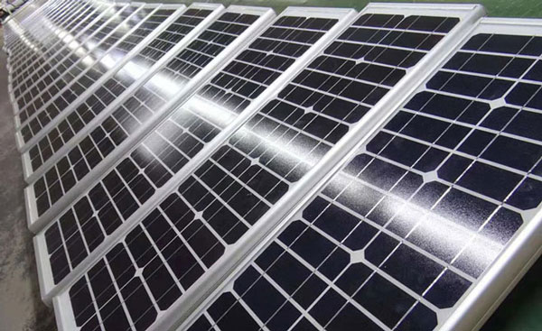
Wafer Slicing
Wafer slicing is a fundamental step in the manufacture of monocrystalline silicon solar cells. In this process, large single crystals of silicon are sliced into thin uniform wafers. The greatest attention in this process is focused on the control of the process guarantees a wafer free of defects and of uniform thickness. The purpose of this note is to introduce the process of wafer slicing and explain how the monocrystalline silicon ingot is turned into a stack of wafers.
Setting Up the Ingot
A cylindrical ingot of monocrystalline silicon is grown using the Czochralski process. The ingot is mounted on a slicing machine, which performs the slicing. The ingot surface is examined and, in some cases, ground. The purpose of grinding is to ensure that the ingot has a perfect, cylindrical shape, and the slicing machine has minimal off-normals in the process of slicing. The off-normal is an inclination of the cutting surface with respect to the saw direction.
Cutting The Ingot
The general technique for slicing the monocrystalline silicon ingot with a multi-wire diamond saw is called wire sawing. In this process, numerous thin wires, approximately 140-160 μ m, are pulled back and forth and cut the silicon. The cutting edge is fed SiC or diamond slurry to ensure that debris is removed and the damage done to the crystal structure is minimal.
Thickness And Precision
The wafers are typically sliced into approximately 200 μ m thick wafers, although the thickness may vary depending on the purpose of the cells. Precision is essential as thickness variations influence implant penetration depths during the doping process and light absorption during the cells operation.
Cleaning and Inspection
The wafers are carefully cleaned to avoid contamination that may influence cell operation with the slicing debris. The cleaning procedure is typically multi-stage, with wafers undergoing several ultrasonic baths in various solvents and high-purity water rinses. The wafer stack is visually inspected for micro-cracks and uniform thickness, but an automatic imaging of the stack may also be employed.
Doping Proce
The doping process is an integral part of the production of monocrystalline silicon solar cells. It is used to introduce impurities energy into the pristine silicon wafers and to create the p-type and n-type semiconductor layers. Each of these is necessary for ensuring operational features of the p-n junction, which is used to convert sunlight into electrical energy.
Purpose of Doping
The process is performed to add very small quantities of specific elements selected to alter the electrical properties of pristine silicon. Most commonly, boron is used for the p-type and phosphorus for the n-type. The dopant and doping level control the amount of charge carriers within the semiconductor, which in turn affects the cell’s efficiency.
Some common methods to perform doping are the following:
Diffusion doping: During this procedure, the silicon wafers are brought in to contact with a psychiatrist of the doodah and left at high temperatures, during which the dope heating silicon diffuses and creates a shallow layer of doped silicone. The depth and concentration of the doping depend on time and temperature. Doping can also occur in the opposite way, gather the substance diffuses from the silicon to the dopant source, which depends on energy, leaving the silicon structure.
Ion implantation: A convenient way to place the dopant in the semiconductor is ion implantation. Ions of the dopant are accelerated in an electric field and implanted into the desired material. The concentration and doping level depend on the dose of imploding ions by kilovolt power that precedes it, which also determines its depth.
Thermal Processing
After the doping, the wafers are subjected to a harsh thermal procedure of annealing. It is performed at very high temperatures and accelerates the healing process: first, it helps to activate the of dropping by letting them reach the desired concentration and fill the lattice spaces of silicon. Different levels of ion activation lead to a change of electrical properties. Not only doping but the player used for ion implantation may create high levels of radiation, which also heals during this process.
Quality Control
Every waver goes through strict quality control after which it is tested with conventional equipment for measurement of its resistivity and carrier concentration. This step is critical since only properly doped wafers will help create an effective p-n junction and high levels of electrical power under sun exposure.
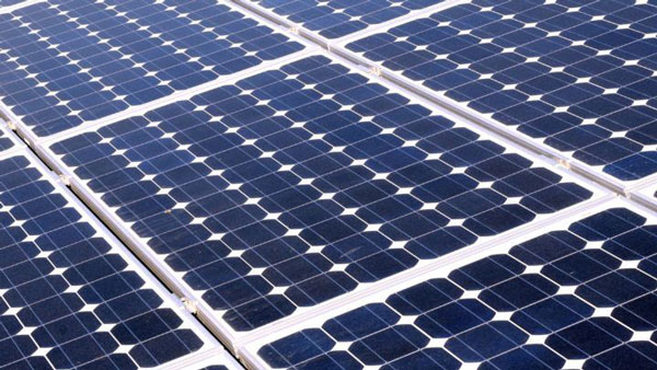
Assembly and Packaging
Assembly and packaging are the final steps in the production of monocrystalline silicon solar cells, crucial for protecting the cells and ensuring their functionality and longevity when deployed in various environments. This phase involves assembling the individual solar cells into panels, wiring them together, and encasing them in protective materials.Cell Interconnection
The process begins with the interconnection of individual solar cells. This is typically done using flat metal conductive ribbons. The ribbons are soldered to the busbars of the cells, connecting them in series to build up the voltage or in parallel to increase the current capacity. Precision in soldering is crucial to minimize resistance and maximize the efficiency of the solar panel.Lamination
Once interconnected, the cells are laminated to protect them from environmental factors such as moisture, temperature fluctuations, and mechanical stress. The lamination process involves placing the interconnected cells between layers of protective materials, usually ethylene-vinyl acetate (EVA) for encapsulation, followed by a layer of durable glass on the front side and a polymer-based backsheet on the rear side.Framing and Sealing
After lamination, the solar panels are framed, typically with aluminum frames. The frames provide structural stability and facilitate the installation and mounting of the panels. Additionally, the edges of the panels are sealed with silicone or other sealing agents to prevent the ingress of moisture and dirt, which could degrade the performance of the solar cells.Electrical Integration and Testing
The final step involves integrating the electrical components, including junction boxes, diodes, and connectors. These components are essential for safely conducting the electricity generated by the panel to the electrical grid or storage systems. Each panel undergoes rigorous electrical testing to ensure that it meets the specified performance criteria. Tests include measuring the output under simulated sunlight conditions, checking for open circuits or shorts, and ensuring the safety and reliability of the electrical connections.Quality Assurance and Packaging
Quality assurance at Dimple Solar involves a comprehensive assembly and packaging procedure. During the assembly, all the panels are assembled in such a way that they will last and will function efficiently. When all of the panels pass all of the quality checks and assessments, they are packaged in the best method possible. That is, the staff at Dimple Solar makes the best to assemble a product by means of qualified workers and equipment so that it lasts and works well. When it comes to qualities of the product which are obtained by means of the packaging procedure, it is essential to state that all of the panels are packaged in such a way as to prevent their damage while in transportation, using appropriate padding and packing supplies. For the work cell, it means that the paper employing in manufacturing or the certain type of wood is used for panels that are much stronger or are less prone to damage. However, for those panels that are especially fragile utmost amends are made so that they suffer no damage during the transportation or handling.
The following text is about doping procedure taking place in the production of monocrystalline silicon solar cells. The following info will prove that doping is required for the overall process and is beneficial for the target item. The text is to define the term given and to introduce to the main types of doping and what it produces.
Definition
Doping is defined as providing impurities to silicon wafers of the total amount of two main types of silicon materials and creation of the p-n junction, which is connected to the effective work of the cell in sunlight. There are a number of ways to supply doping to pure silicon. As for benefits of the given procedure, it is essential as far as there is a necessity to manufacture effective solar cells on the one hand and to employ different basic dopants during the process of manufacturing to obtain n-type silicon. The main type to supply pure silicon with boron impurities is often referred to as p-type silicon.
Types
There is a wide range of types to mention: diffusion and ion implantation, or ways of delivering impurities to silicon wafers: solid-source diffusion, spin-on-glass sources, or in-situ doping. All of these types vary in time, temperature and other factors to use during the process. As for the final product, the concentration of the perfect dopant and the best way to introduce a type of impurities determine the exact charge carrier concentration in the semiconductor product.
After effects
As long as silicon is doped, thermal annealing has to be performed. It is essential in that it has to be at a high enough temperature and answer one major need – the silicon must form a structural site in the silicon lattice. Thus, silicon wafers have changed electric properties. Another essential factor is that the potential lattice damage which has occurred in the silicon during the doping process has to be healed.