Introduction
Silicon is the essential part of the modern electronics production. The process of its extraction and refinement is the interesting way from the earth to the narrow wires of the microchips that started a new era of the modern electronics. This paper will discuss the sources of silicon and abundance of this element, as well as the process of mining and the refinement of silicon.
Sources of Silicon: Mining and Refinement
Silicon is the second element after oxygen, which is found in the earth crust in the biggest quantity. According to the United States Geological Survey, silicon accounts for a total of 27.7% of the weight of the earth crust. The main sources of silicon are sandstone and quartz, which are mined all over the world. The process of mining is rather simple and includes the open-pit mining or the underground mining of silicon-rich materials.
It must be noted that the mining process is rather expensive and includes the highly technical procedures. After the raw materials are mined, they are first delivered to the nearby processing factory. It starts with the crushing and grinding of raw materials. The next step is the froth-flotation in the tanks. It allows the raw materials to be more purified, the result of which is that silicon dioxide is removed from the other ores in the form of froth. It must be noted that the gas is further purified to yield the high-quality silicon. The center of the silicon mining is thus, the reduction of quartz to metallurgical grade silicon, while using carbon at higher temperature.
The metallurgical-grade silicon is then further refined through a series of chemical reactions to produce industrial-grade silicon. The process involves the use of chlorine gas and hydrogen gas in a series of reactions that result in the production of TCS, which is then reduced to produce high-purity silicon.
Steps to Create Industrial-Grade Silicon
Creating industrial-grade silicon involves a multi-step process that begins with the production of trichlorosilane. The is then subjected to a process known as Chemical Vapor Deposition. The silicon is then formed into polycrystalline ingots, which are then sliced into wafers. These wafers become the primary material for the production of semiconductor devices and solar panels.
Purification into Electronic-Grade Silicon
The final step in the silicon production process is the purification into electronic-grade silicon. This is a crucial step as the silicon’s purity is directly related to the performance of the electronic devices it will be used in. The purification process is a series of chemical and physical steps that remove trace impurities, resulting in purity of 99.999999% or higher.
The purified silicon is then ready to be used in the production of allowed semiconductor devices, the key components of modern electronics. From smartphones to supercomputers, this high-purity silicon is the backbone of the devices that define our era.
Solar energy is one of the fastest-growing renewable energy sources, and silicon is a key technological element for its installation. Understanding the journey of silicon through solar panel manufacturing reveals the critical place of this element. Though this paper, it was discovered that silica is an apt element for solar cells, which convert sunlight to energy in all matters of uses. The importance of the place was explored: it is possible to convert sand to silicon wafers, and these wafers may be used as solar panels in households and multiple other destinations. Thus the place of silicon as a material for solar panels was determined and effectively used.
Solar Cells: How & Why
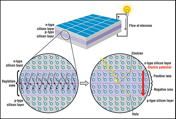
Solar cells, usually called photovoltaic cells, are essential to convert sunlight into electricity. The most common material used for their production is silicon because it has specific semiconducting properties that are useful in creating this connection: silica is able to absorb energy from sunlight and turn it into an electrical current. The majority of solar cells are made of monocrystalline silicon or polycrystalline silicon: the first type is more effective and has a number of advantages, the percentage of their efficiency is 20%, and the second type is more accessible, though has an effectivity level of only 15-16%. It is important to emphasize the silicon wafers are used in manufacturing of solar panels that are commonly used in similar manners.

Sand to Wafer: Solar Cell Material
The primary use of silicon for multiple uses, including solar cells, begins with sand first mined from the abode of the Earth. The sand is put into an electric arc furnace, which heats it to generate metallurgical-grade silicon, which varies greatly from solar-grade silicon. This is one of the steps in a production process using a TCS (trichlorosilane) method.
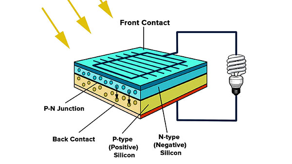
Then the high-purity silicon is re-melted and discharged in the forming crucible, being solidified in the monocrystal silicon ingot. The ingot is sliced with the use of a wire saw or laser cutting. Sliced silicon wafers, which are stacked and connected in a certain way, form a solar cell. The cell is laminated with a layer of glass and the rear surface is also protected with some durable material, to form a module. The modules are then connected in series or parallel to finally form a solar panel being mounted on a base construction to catch the sun. Thus, the travel of silicon from sand to solar panel is one of the most sophisticated ones and displays the elaboration of the renewable energy industry.
However, in general, the increased demand for renewable types of energy products and the transition to an environmentally friendly energy system means that humanity will increasingly depend on silicon and the peculiarities of solar panel manufacture for a long time. At the same time, modern solar panels are complex engineering constructions, so their efficiency and life do not depend only on the purity of the silicon used, and a range of other materials and components are used in their construction. Let us, therefore, consider other materials and advanced technologies used to enhance the efficiency of solar panels.
The role of other materials in photovoltaics
Even though silicon occupies the most important place in a solar cell, using other materials is not almost less important. For example, some metal contacts are necessary to ensure electron flow in the upper and lower part of the cell. Silver is used to manufacture these contacts, as it is a perfect conductor of electricity, and it also does not bother with outdoor conditions.
Apart from the solar cells, another major component is the encapsulant, which is usually made of ethylene-vinyl acetate or polyvinyl butyral. This thermoplastic is used to seal the solar cells in the panel to protect them from environmental factors such as moisture, dust, and UV light. Thus, this material is highly important for the performance and longevity of the solar module, as it holds the individual cells and the glass together. Moreover, since the glass has to protect the cells, it cannot be dense and must be as transparent as possible: it is usually tempered due to its strength and thermal stress resistance.

Advanced Technologies Enhancing Solar Efficiency
The efficiency of solar panels is an important matter, and the industry develops new technologies to make them generate more power with a limited surface area. For example, passivated emitter and rear cell technology involves a special layer of material on the rear of the solar cell, which reflects the particles of light that have not been absorbed in the silicon back into the material, increasing the probability that it can generate electricity. As much as 20% more energy can be produced using this technology when compared to the traditional cells. Multi-junction or tandem solar cells are designed with multiple layers of different semiconductor material: each layer is attuned to a different part of the solar spectrum, and their overall efficiency is vastly superior, as each photon can trigger the creation of more than one electron. Moreover, more and more bifacial solar panels which can absorb the light from both sides of the unit are being used, making it more efficient where the ground or the roof is covered with white snow, reflecting the sunlight.
Besides, to make the silicon solar cell work better and give the new impulse to its wide-scale implementation, the new materials, particularly perovskite, are used. For example, stacked perovskite on crystalline silicon solar panels produce a conversion efficiency of 30% or so as against of that of the silicon panel alone of not more than 19%; thus, this covers the market niche that serves as a foothold for further improvement. Moreover, the use of the silicon-based tandem photovoltaics assumes that the radiation passes through the crystalline silicon and is converted into electricity by the perovskite slab placed on top of it. It is notable that because perovskite captures minimal light at specific wavelengths, the range of its application is rather limited for a present moment; however, this serves a starting point for the further implementation of innovations. In addition, MLPE such as microinverters or power optimizers are used to get the maximum output of each panel by every solar panel functioning optimally. As the technology impacted almost just about every aspect of life regarding labour productivity as well as life expectancy, prolonging the operation of solar panels and minimizing their immediate costs, and increasing their effectiveness is just a beginning which promises other surprises in the future!